Processes
PECVD
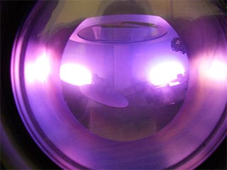
 Plasma Enhanced Chemical Vapor Deposition (PECVD) is a low pressure deposition process that uses plasma as an assisting means to produce solid films onto a substrate from a gas or vapor source. Plasma is used to generate the radicals that participate in the film growth and allows for a “low” temperature process when compared to standard CVD processes.
MVSystems uses a capacitive configuration (i.e. parallel plates) to generate the plasma. The substrate is connected to a ground electrode while the other plate (electrode) is powered by a DC, RF or VHF source. RF (13.56MHz) is the most commonly used type of excitation.
Among other innovations, MVSystems developed the pulsed PECVD (P-PECVD) technique which uses a modulation frequency in the 1-100kHz range to improve deposition rate of high quality film materials. The introduction of a periodic OFF time during the process is the key to allowing higher power input without deleterious effects on the properties of the film.
HWCVD
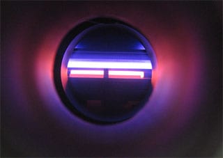
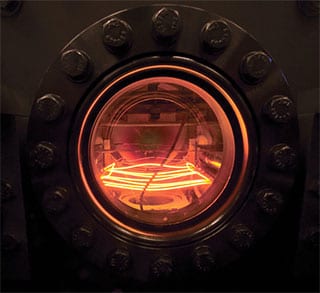 Hot Wire Chemical Vapor Deposition (HWCVD) or Catalytic Chemical Vapor Deposition (CAT-CVD) is a process in which the reactant gases are decomposed via catalytic or pyrolytic reactions by a heated catalyzer. This method has been successfully used to produce high quality silicon-based thin films such as amorphous-silicon (a-Si:H), nanocrystalline-silicon (nc-Si) and silicon nitride (a-SiNx:H).
Among the advantages of using HWCVD are the possibility of introducing a low concentration of hydrogen in the silicon based alloys, potential for high deposition rates and the possibility of producing high quality films at low temperatures.
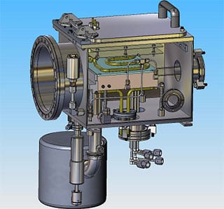
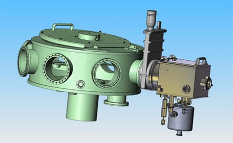
MVSystems offers standalone single chambers as well as modular processing chambers that can be integrated to our cluster tools. Filament materials from tantalum and tungsten to graphite can be used. The hot wire assemblies can be supplied with substrate to filament distance adjustment. Heated and cooled substrate holders are available.
SPUTTERING
 Sputtering, like the other processes described in this section, is a low pressure thin film deposition process. Differently from CVD, however, the source material in this case is a solid, not a liquid or a gas. In sputtering, particles from the solid source (or target) are extracted by the bombardment of energetic particles created in a plasma. The sputtered atoms from the target travel through the plasma in front of the target and those atoms that reach the substrate form the thin film. In order to generate the bombardment described above, the target is electrically charged using typically DC, pulsed-DC or RF power supplies. The choice of type of excitation source depends on the type of material being deposited, deposition rates required, type of gas(es) used (reactive or not), etc. The detailed description of all components and mechanisms involved in sputtering process is outside the scope of this section but is abundantly available in the literature.
MVSystems routinely provides standalone systems and modular units incorporated to its cluster tools. Processes for the deposition of metals, dielectrics, transparent conducting oxides, such as Al-doped zinc oxide (AZO) and indium tin oxide (ITO) and novel transparent semiconductor materials such as (ZnON) are available.
Thermal Evaporation
 Thermal evaporation typically uses a resistive heat source to evaporate a solid material in a vacuum environment. The evaporated material that reaches the substrate condenses to form the thin film. The more common use of thermal evaporation involves the deposition of single metallic materials such as silver or aluminum to be used as electrical contacts. In more complex applications (functional films) the co-deposition of several components can be achieved via careful control of the temperature of individual crucibles, for examples when depositing Cu-In-Ga-Se alloys.
MVSystems provides standalone evaporation systems and modular units incorporated to its cluster tools.
Atomic Layer Deposition
Atomic Layer Deposition (ALD) addresses the need for nanometers thick, pinhole-free films with a high-degree of conformity regardless of the geometry. Industry applications for ALD include semiconductors, MEMS, photovoltaics energy storage, lighting, and more.
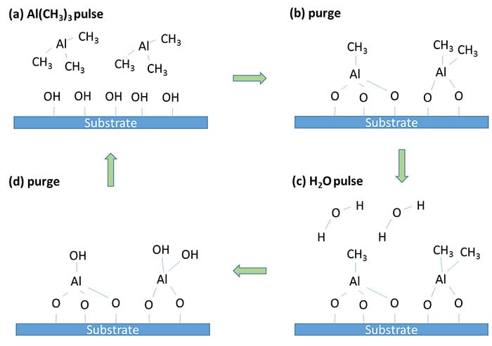
ALD films grow in atomic monolayers through chemical half reactions minimizing pinholes and maximizing film thickness uniformity. The growth of Al2O3 from water (H2O) and trimethylaluminum (TMA) can be used to explain the principles behind ALD. The substrate is hydroxylated from exposure to air or oxygen. The first TMA precursor pulse reacts with the OH groups at the surface of the substrate creating the first Al monolayer with CH3 bonds remaining exposed. After the TMA precursor, a purge pulse of inert gas removes any remaining TMA precursor gas from the reaction cell. After the purge cycle, an H2O pulse removes the CH3 bonds leaving OH bonds again on the surface. A purge pulse removes any remaining H2O within the chamber. These steps form a cycle which is repeated to achieve the necessary thickness.
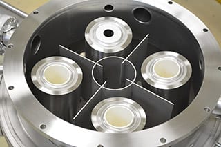
MVSystems’ ALD system can either be used as a standalone chamber or mounted as a modular processing zone (MPZ) to a cluster tool. The system consists of an outer vacuum chamber and an inner reaction cell. This design allows for a small reaction zone volume and uniform heating of the substrates.