Sputtering
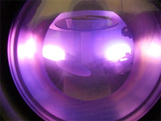 Sputtering, like the other processes described in this section, is a low pressure thin film deposition process. Differently from CVD, however, the source material in this case is a solid, not a liquid or a gas. In sputtering, particles from the solid source (or target) are extracted by the bombardment of energetic particles created in a plasma. The sputtered atoms from the target travel through the plasma in front of the target and those atoms that reach the substrate form the thin film. In order to generate the bombardment described above, the target is electrically charged using typically DC, pulsed-DC or RF power supplies. The choice of type of excitation source depends on the type of material being deposited, deposition rates required, type of gas(es) used (reactive or not), etc. The detailed description of all components and mechanisms involved in sputtering process is outside the scope of this section but is abundantly available in the literature.
MVSystems routinely provides standalone systems and modular units incorporated to its cluster tools. Processes for the deposition of metals, dielectrics, transparent conducting oxides, such as Al-doped zinc oxide (AZO) and indium tin oxide (ITO) and novel transparent semiconductor materials such as (ZnON) are available.