Atomic Layer Deposition
Atomic Layer Deposition (ALD) addresses the need for nanometers thick, pinhole-free films with a high-degree of conformity regardless of the geometry. Industry applications for ALD include semiconductors, MEMS, photovoltaics energy storage, lighting, and more.
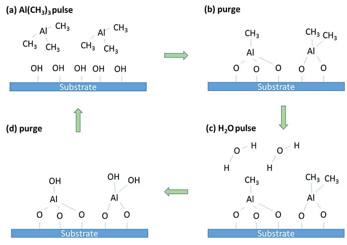
ALD films grow in atomic monolayers through chemical half reactions minimizing pinholes and maximizing film thickness uniformity. The growth of Al2O3 from water (H2O) and trimethylaluminum (TMA) can be used to explain the principles behind ALD. The substrate is hydroxylated from exposure to air or oxygen. The first TMA precursor pulse reacts with the OH groups at the surface of the substrate creating the first Al monolayer with CH3 bonds remaining exposed. After the TMA precursor, a purge pulse of inert gas removes any remaining TMA precursor gas from the reaction cell. After the purge cycle, an H2O pulse removes the CH3 bonds leaving OH bonds again on the surface. A purge pulse removes any remaining H2O within the chamber. These steps form a cycle which is repeated to achieve the necessary thickness.
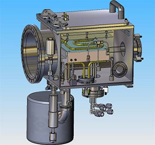
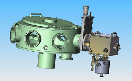
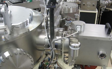
MVSystems’ ALD system can either be used as a standalone chamber or mounted as a modular processing zone (MPZ) to a cluster tool. The system consists of an outer vacuum chamber and an inner reaction cell. This design allows for a small reaction zone volume and uniform heating of the substrates.